
File:Cmos-chip structure in 2000s (en).svg

此SVG文件的PNG预览的大小:407 × 599像素。 其他分辨率:163 × 240像素 | 326 × 480像素 | 521 × 768像素 | 695 × 1,024像素 | 1,390 × 2,048像素 | 550 × 810像素。
原始文件 (SVG文件,尺寸为550 × 810像素,文件大小:138 KB)
摘要
| 描述 |
Català: Estructura esquemàtica d'un xip CMOS, tal com es va construir a principis dels anys 2000. El gràfic mostra els LDD-MISFET sobre un substrat de silici SOI amb cinc capes de metal·lització i un tap de soldadura per a la unió de xip. També mostra la secció per a FEOL (front-end de línia), BEOL (back-end de línia) i les primeres parts del procés de back-end. (versió traduïda a l'alemany)
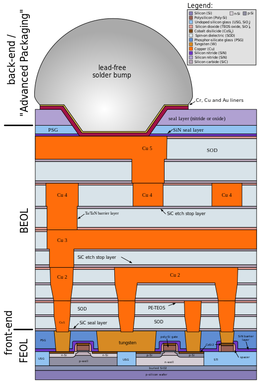
English: Schematic structure of a CMOS chip, like it is built in the early 2000s. The graphic shows LDD-MISFET's on a SOI silicon substrate with five metallization layers and solder bump for flip-chip bonding. Also it shows the section for FEOL (front-end of line), BEOL (back-end of line) and first parts of back-end process. (translated German version) |
| 日期 | 2006年12月9日 (上传日期) |
| 来源 | self made (from university scripts and scientific papers) |
| 作者 | Cepheiden |
| 其他版本 |
Other related versions:[]
|
.svg&lang=ca)
.svg&lang=en)

.svg)
.svg?uselang=zh)
.svg?uselang=zh)
.svg?action=history&uselang=zh)
.svg)
.svg)
|
此SVG檔案包含可翻譯至您的語言的内嵌文字,可以使用任何可用SVG編輯器、文本編輯器或SVG翻譯工具來翻譯。詳情請見:關於翻譯SVG檔案。 |
.svg)
此檔案使用SVG <switch>元素翻譯。所有的譯文都儲存在同一檔案中!了解更多。
請在 要將此檔案中的文字翻譯成您的語言,您可以使用SVG 翻譯工具。或者,您可以將該檔案下載至您的電腦中,使用您熟悉的任何軟體進行翻譯,然後使用「相同」名稱重新上傳。如果不確定如何進行此操作,您能在圖像實驗室中找到幫助。 |
许可协议
我,本作品著作权人,特此采用以下许可协议发表本作品:

|
已授权您依据自由软件基金会发行的无固定段落及封面封底文字(Invariant Sections, Front-Cover Texts, and Back-Cover Texts)的GNU自由文件许可协议1.2版或任意后续版本的条款,复制、传播和/或修改本文件。该协议的副本请见“GNU Free Documentation License”。 |
| 本文件采用知识共享署名-相同方式共享 3.0 未本地化版本许可协议授权。 | ||
| ||
| 本许可协议标签作为GFDL许可协议更新的组成部分被添加至本文件。 |
您可以选择您需要的许可协议。
文件历史
点击某个日期/时间查看对应时刻的文件。
| 日期/时间 | 缩略图 | 大小 | 用户 | 备注 | |
|---|---|---|---|---|---|
| 当前 | 2024年2月5日 (一) 14:35 | | 550 × 810(138 KB) | Manlleus | File uploaded using svgtranslate tool (https://svgtranslate.toolforge.org/). Added translation for ca. |
| 2024年2月5日 (一) 14:25 |  | 550 × 810(97 KB) | Manlleus | fixed text labels for translation | |
| 2006年12月9日 (六) 18:52 |  | 550 × 810(85 KB) | Cepheiden | {{Information |Description= Schematic structure of a CMOS chip, like it is build in the early 2000s. The grafic shows LDD-MISFET's on a SOI silicon substrate with five metallization layers and solder bump for flip-chip bonding. Also it shows the section f | |
| 2006年12月9日 (六) 18:49 |  | 550 × 810(85 KB) | Cepheiden | {{Information |Description= Schematic structure of a CMOS chip, like it is build in the early 2000s. The grafic shows LDD-MISFET's on a SOI silicon substrate with five metallization layers and solder bumb for flip-chip bonding. Also it shows the section f |
文件用途
全域文件用途
以下其他wiki使用此文件:
- ar.wikipedia.org上的用途
- ca.wikipedia.org上的用途
- en.wikipedia.org上的用途
- fa.wikipedia.org上的用途
- fi.wikipedia.org上的用途
- hy.wikipedia.org上的用途
- id.wikipedia.org上的用途
- ja.wikipedia.org上的用途
- ko.wikipedia.org上的用途
.svg)